IBM I/O Technology Department
I was hired by the IBM Research Division after completing the RCA Institute T3 course. The course consisted of the majority of math, physics and electronic engineering courses in the New York Polytechnic BSEE program.
Holographic fabrication of crystallographically aligned sub-micron gratings in GaAs
When I was hired by IBM I was assigned to Peter Zory as his lab tech. After building a dye laser for the IC personalization system he had designed I was put to work on his pet project. This required that a second order diffraction grating be made in the contact layer of a DH AlGaAs laser diode. The thesis was that the grating would provide both (distributed) feedback and a large output aperture. This would come close solving the problem of large beam divergence and, perhaps reducing the heat problem by reducing the lasing threshold current.
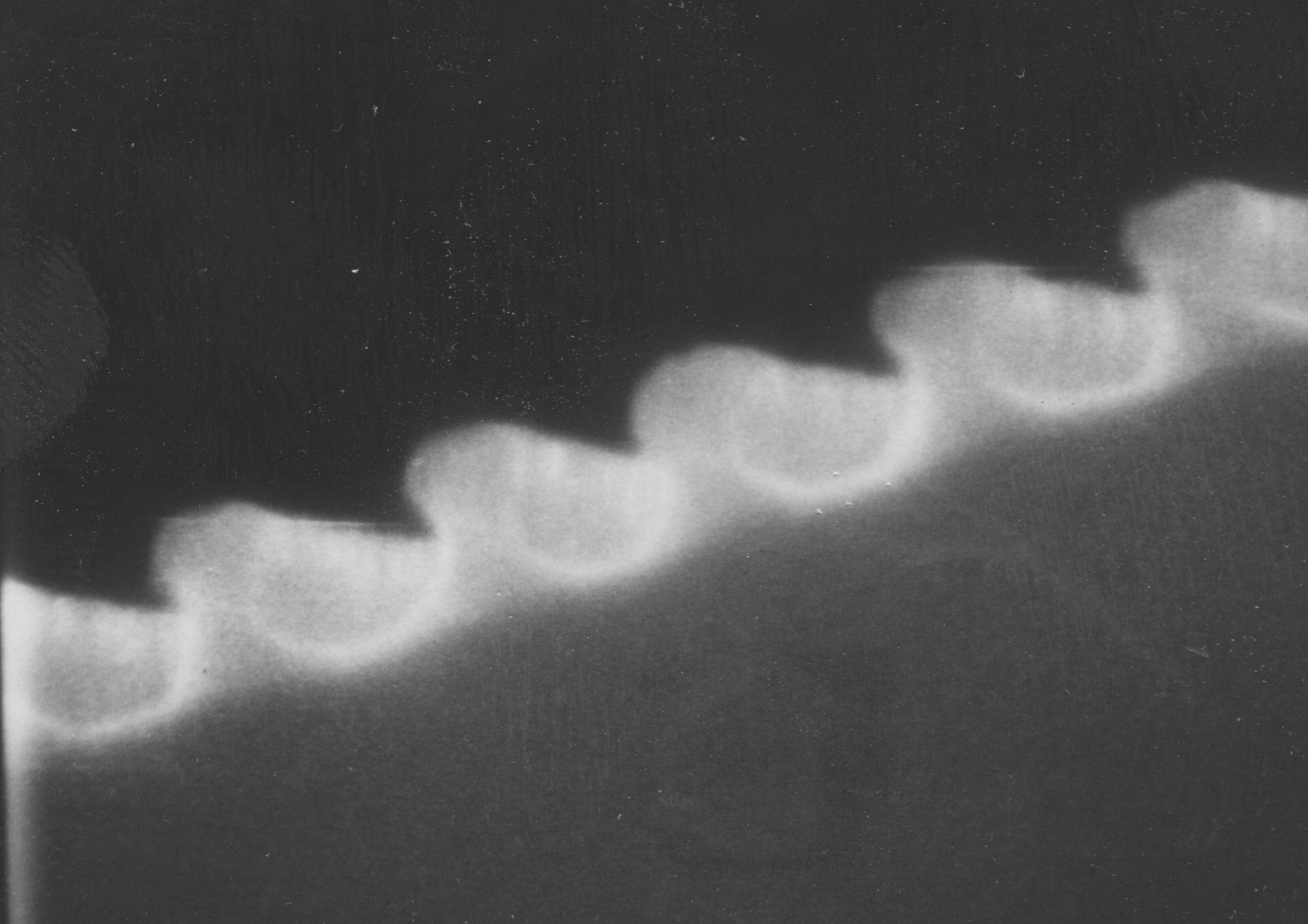
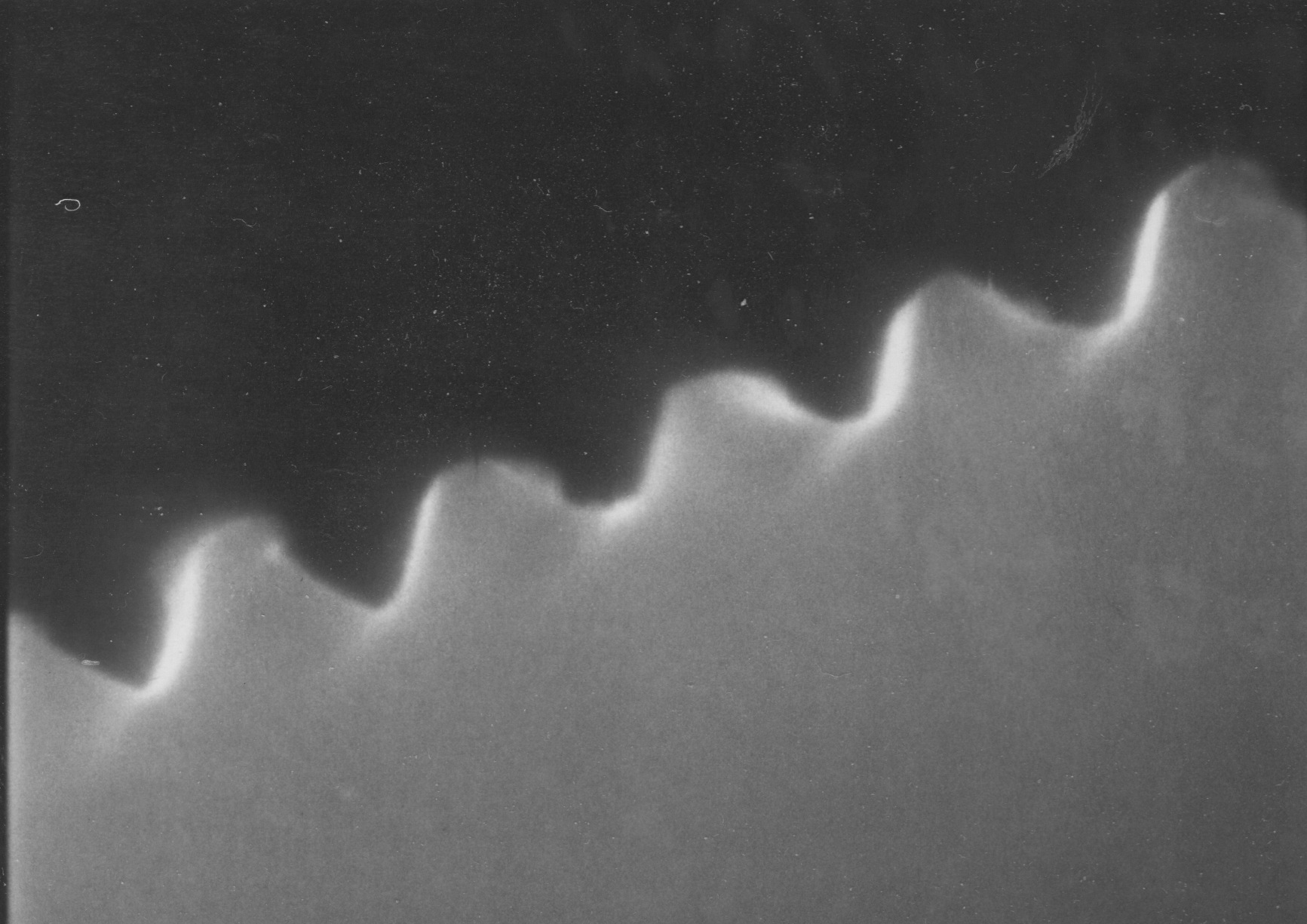
My role in this project was to develop the processes and perform the fabrications needed to test Dr. Zory's ideas. I developed the apparatus needed to make crystallographically aligned holographic diffraction gratings on small pieces of unprocessed laser wafer (provided by the DH Laser Group. This required making very thin photoresist layers on surfaces without creating pin holes. The thin layers were needed to assure that photoresist developed through to the laser wafer surface. The film could then be exposed in the interferometer, developed, post processed with an off-axis metal evaporation and etched in a preferential etchant. The electron microscope photos below (taken by Oliver Wells) show cross sections of a photoresist diffraction grating mask (left, slightly underdeveloped) and a cross section of a diffraction grating etched through such a mask (right, after the mask was stripped). The grating period is about 2400 Angstroms which means the distance from groove center to center is about 425 atoms.
|
|
Grating Coupled Semiconductor Laser Diodes
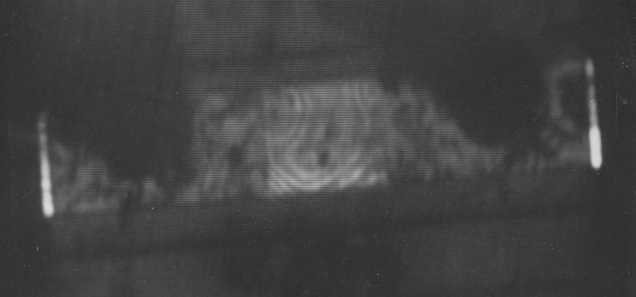
For the last stage of the process I developed the method for fabricating laser diodes from the processed wafer. We were successful in making grating coupled laser diodes but it didn't solve the problems we had hoped it would. The infrared microphotograph below show a functioning grating coupled laser diode from above. The central square (showing an interference pattern) is the grating coupler.
|
Pete told me that if I participated in writing a journal article for this work I would have first author position on the grating fabrication article and second on the device physics article. I think of it as a measure of Pete's intellectual integrity that he didn't just "acknowledge" me at the end of the article. I've been told that after this work my reputation was that I could be given a hard problem and left alone, and that after a while I would come back with something that worked. I owe Pete a great deal.
Semiconductor Lasers on Silicon Optical Benches
The Silicon Optical Bench was a successful attempt to solve two problems with the DHS semiconductor laser: the devices had to dissipate as much as a watt of heat from a volume that measured about 100 cubic microns and the devices had a highly divergent beam in one axis. The emitting aperture of the device had to be aligned with sub-micron accuracy to an optical collection system designed to compensate for the divergent beam pattern of the laser.
This work could not have been accomplished without the contributions of John Harper (optical design) and Michael J. Brady (Silicon Optical Bench fabrication). Credit for the initial concept was claimed by Eric Lean (Manager) and John Crow (RSM). Robert Laff (RSM) developed a thermal resistance model of the laser diode / silicon / copper package.
My roll in this project included developing the technique for removing laser dice of controlled size from wafers of laser material, Developing low thermal resistance, low stress bonding techniques and machinery for attaching laser dice and laser arrays to SiOB's. Once I had solved the packaging problem I continued to work on test and application, developing electronic control systems for laser diodes, developing complete optical transmitters and receivers for optical data links, developing driver/controllers for high powered laser diode packages, developing thermally accelerated aging systems (which led to my developing a set of standards for selection of potentially long lived diodes, and developing several forms of optical connectors and switches.
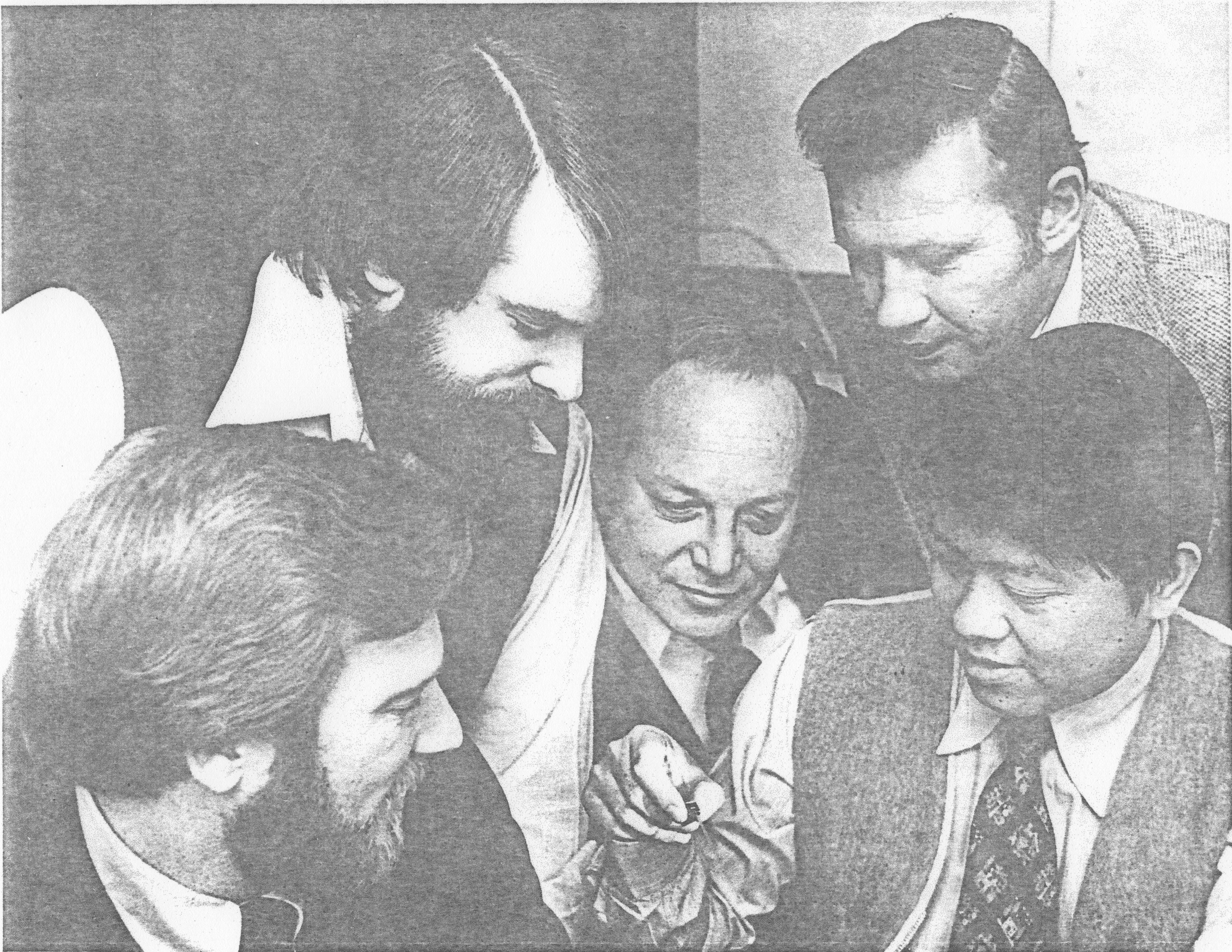
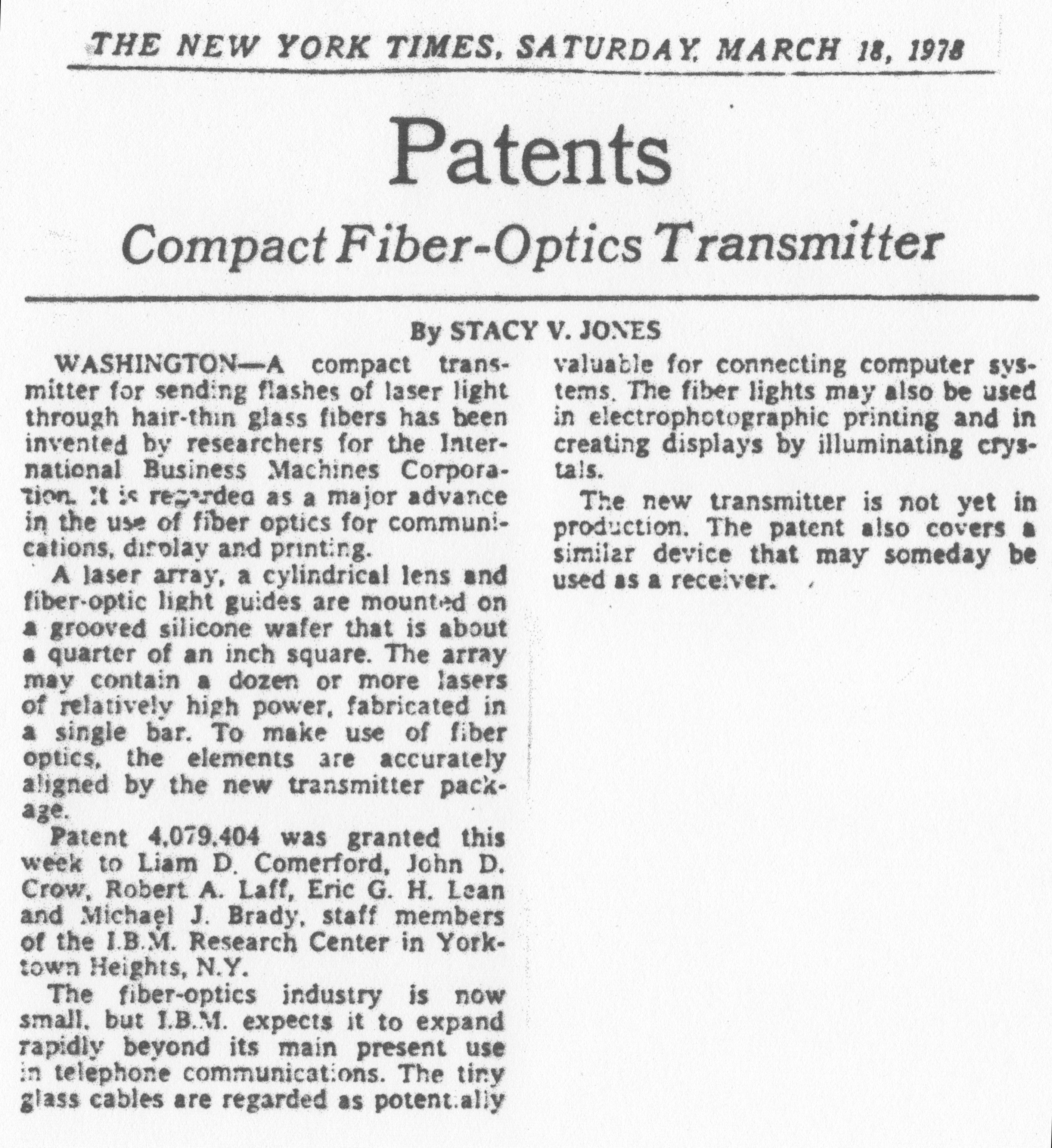
The work was documented in journal and conference papers. Eventually the work was used for IBM publicity. Here is the article and photo by the NY Times. When it appeared in the Times it was cropped so that only the lower right corner was shown. I'm the guy in the upper left corner. John Harper didn't get in the picture at all.
|
|
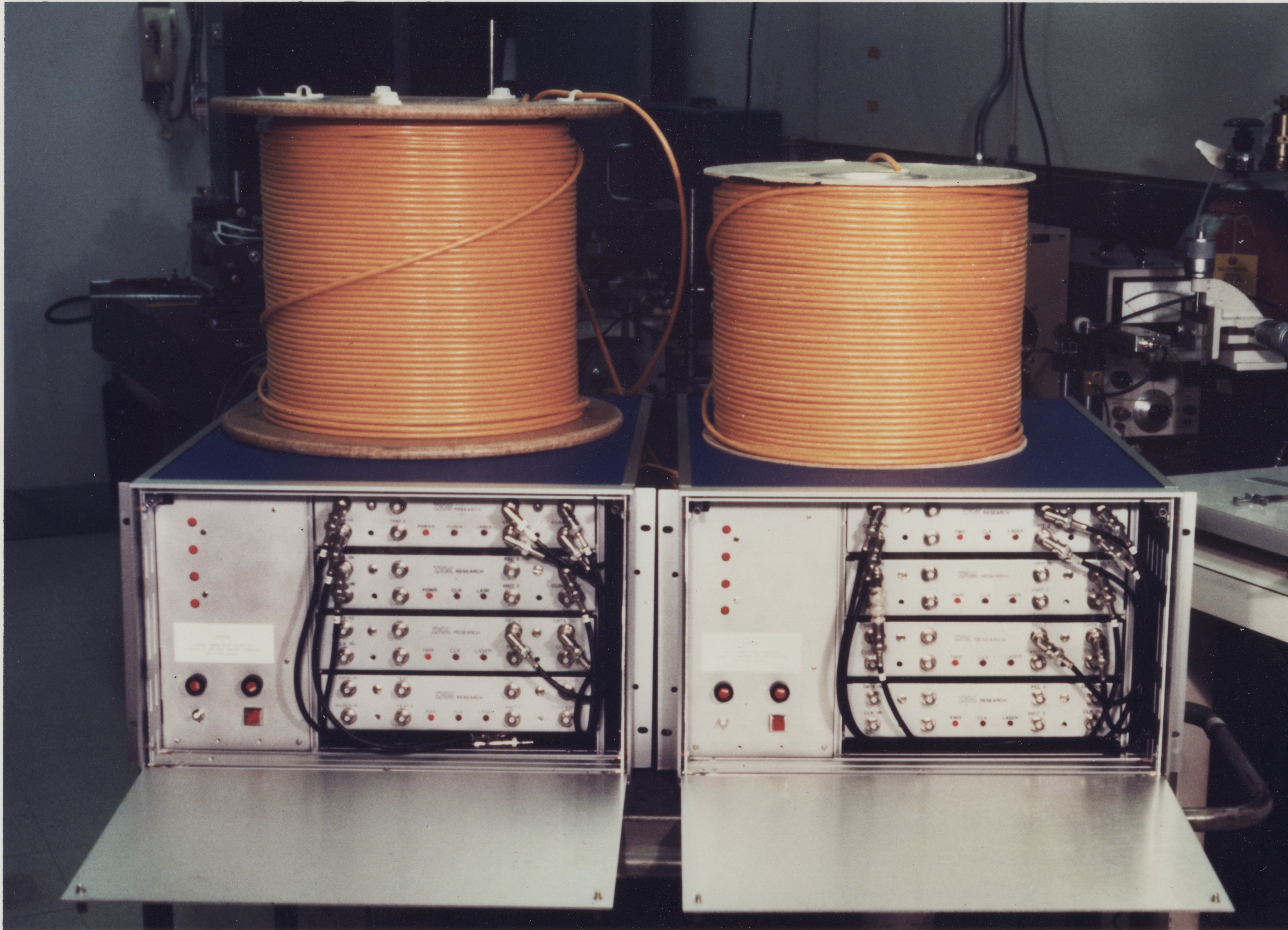
The 801 Optical Data Link
I used the laser packages that I designed, built and burned in to build several fiber optic data links. These included the data link for the 801 Minicomputer, the first RISC system. This system used the System 370 in the computing center as its I/O processor. The 801 Optical Data Link (shown below) was used to connect the 801 Mini to the System 370 located about a half kilometer away. Specifications for the link included first-bit-sent acquisition of the data clock at any data rate from 0 to 50 Mbit/sec. I designed and built the coding system (which operated at 0 to 100 Mbit/sec), invented and built the optical connectors, designed and built the optical receivers and transmitters, invented and built the laser bias control system, built the link hardware, and demonstrated its operation at Bit Error Rates much less than ten to the minus twentieth errors per second.
|
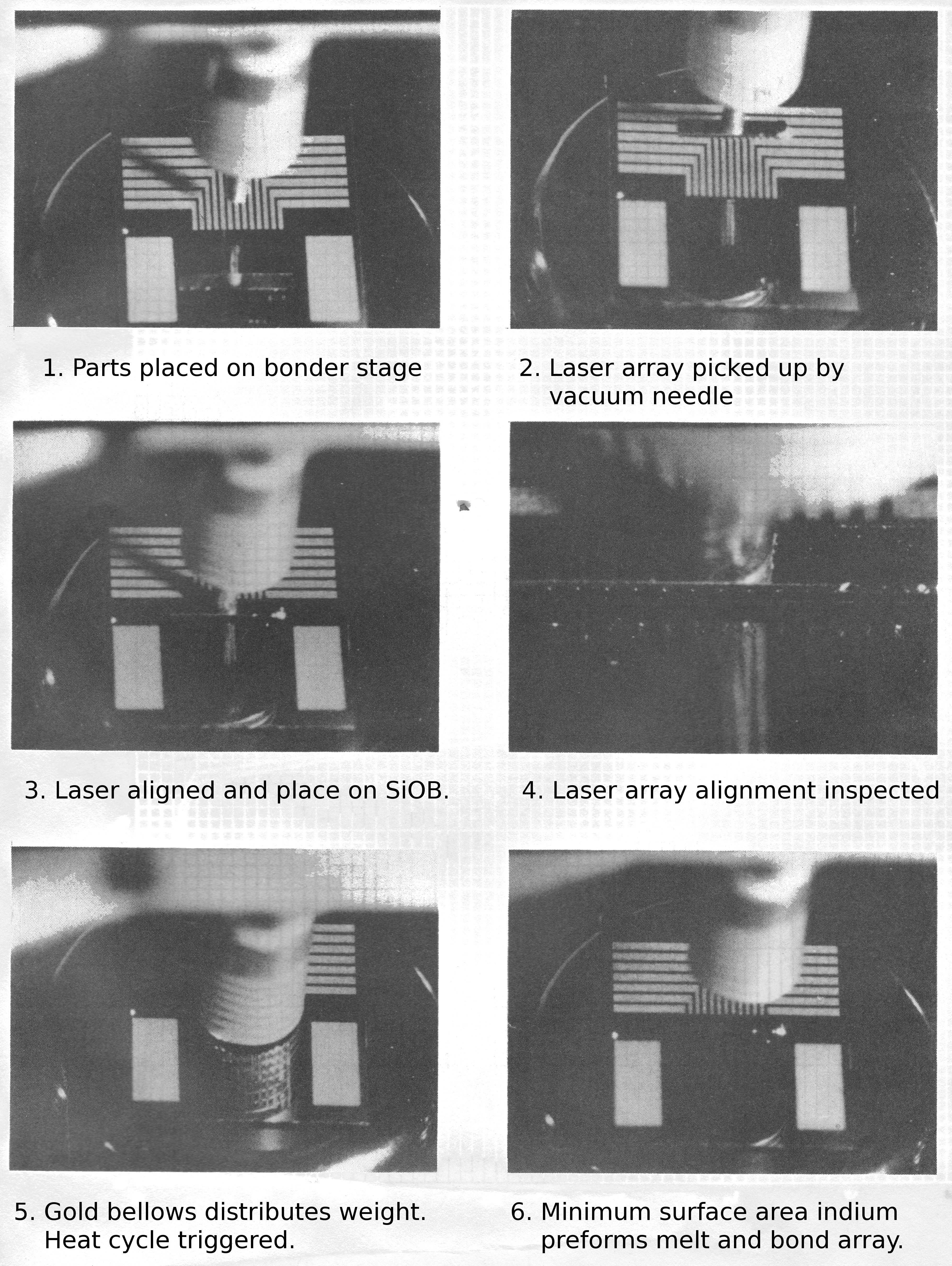
Monolithic Laser Arrays on Silicon Optical Benches
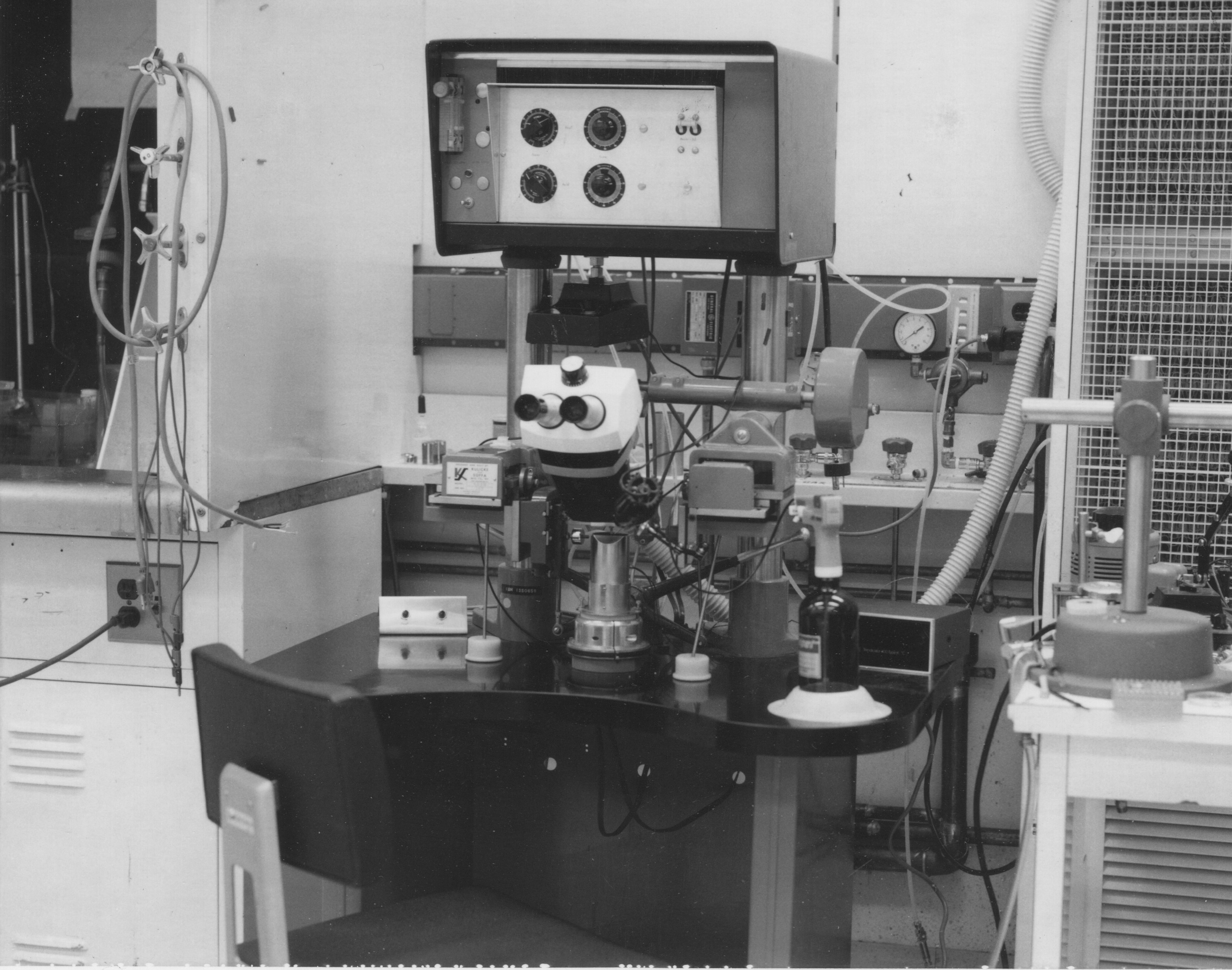
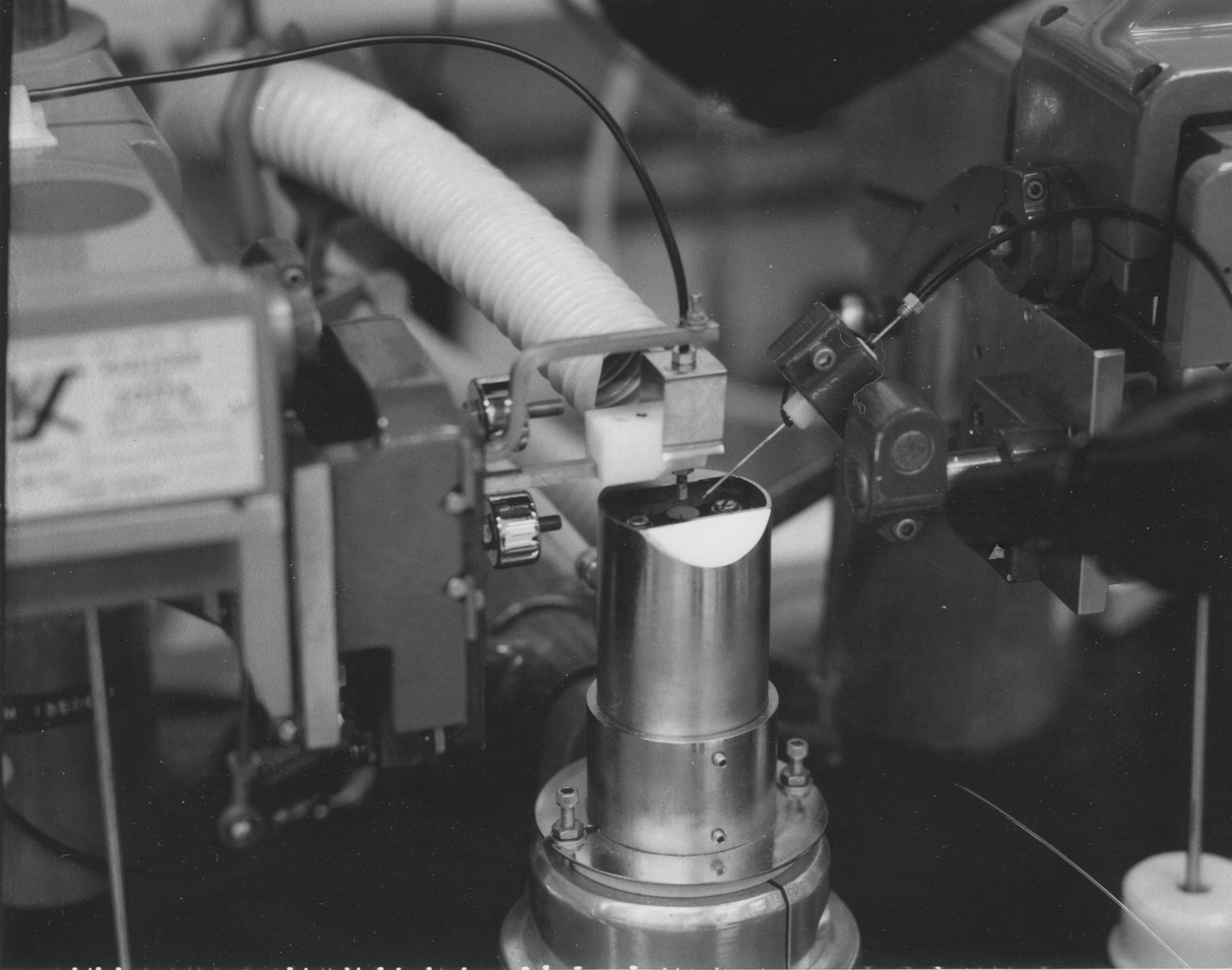
Laser diodes could also be harnessed for printing and large area computer displays. Research on the printing and display applications took place at other locations. I developed the technology needed to bond monolithic arrays of lasers onto SiOB's and supplied these to the efforts in the printing and display divisions of IBM.
The photos below show (left to right, top to bottom) the laser bonder, the bonding stage, the sequence of the array bonding process and a completed laser diode array package. In bonder in the first photo is built on an old thermo-compression wire bonder loaned to the project by Lars Osterling (and Leo Esaki). I stripped out the electronics and the bonding apparatus (leaving the micro-manipulators and microscope mount) and replaced them with a controller and bonding system that I designed and built. The same apparatus, was used for bonding single laser diodes by means of a capillary reflow on SiOB process I developed. Those devices were used in the 801 Optical Data Link shown above.
|
|
|
|
Over the course of my work with AlGaAs lasers I received awards, was issued patents and published in journals. I was promoted rapidly. A few years after being promoted to Research Staff Member (called "Staff Scientist" everywhere but IBM) I told my management that I really had no interest in the field. I was given my choice of areas in which to work.
Return to the Home Page